Nationwide Momentum in Chip Design as India Prepares Workforce for AI Age: Shri Ashwini Vaishnaw
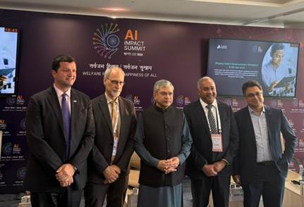
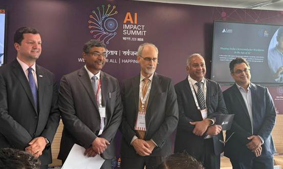
The session “Semiconductor Workforce in the Age of AI” at the India AI Impact Summit 2026 positioned talent development as the decisive link between India’s artificial intelligence ambitions and its semiconductor manufacturing roadmap. Bringing together leaders from government, industry and academia, the discussion underscored that the next phase of India’s semiconductor journey will depend not on incremental skilling initiatives, but on building a deep, end-to-end understanding of the fab ecosystem, spanning device physics, process integration and advanced manufacturing systems.
In his keynote address, Shri Ashwini Vaishnaw, Union Minister for Electronics and Information Technology, outlined the national vision for creating a globally competitive semiconductor ecosystem and strengthening India’s long-term position in the AI value chain. He said, “From Assam to Jammu and Kashmir, from Kerala to Tamil Nadu, students across nearly every part of India are now designing chips themselves. In this AI-driven age of intelligence, semiconductors will be one of the most critical layers of our technology architecture, and this capability will become a major national strength for many years to come.”
Shri S. Krishnan, Secretary, Ministry of Electronics and Information Technology, highlighted the strategic convergence of the India AI Mission and the India Semiconductor Mission, emphasising the need to move from design leadership to manufacturing scale. He said, “This session represents the convergence of India’s two major missions: the India AI Mission and the India Semiconductor Mission. Semiconductors are central to the AI story, just as AI is increasingly central to the semiconductor story. For India to be a reliable, long-term partner, it is vital that we move beyond design, where we already contribute 20% of the world’s semiconductor design team, to become a leader in advanced manufacturing. We have already committed to 10 major semiconductor plants across the country. At least four will commence production during 2026, with the remaining following in due course. Furthermore, the India Semiconductor Mission 2.0 will cover the entire ecosystem, including the domestic manufacture of semiconductor equipment.”
The panel discussion that followed reframed workforce development as an ecosystem challenge rather than a training problem. Speakers emphasised that in an industry defined by extreme precision and long learning cycles, isolated skill acquisition is insufficient. What is required is a generation of engineers and technicians who understand not only how tools operate, but why processes behave the way they do across the fabrication chain.
The session brought together David Fried, Corporate Vice President, Lam Research; Paul Triolo, Partner, DGA Group; Saurabh Chandorkar, Associate Professor, Centre for Nano Science and Engineering, IISc, reflecting a shared recognition that human capital will determine the pace and credibility of India’s semiconductor expansion.
Industry leaders noted that while global semiconductor hubs built their capabilities over five to seven decades, India is attempting to compress that journey into a much shorter timeframe. This acceleration, they argued, is possible only through tightly integrated collaboration between academia, equipment manufacturers and fabrication facilities, with curriculum, research and hands-on training aligned to real production environments.
The IISc “SemiFirst” collaboration with industry was highlighted as a working model for this approach. By combining simulation-led learning with exposure to real fab subsystems, such as pressure gauge systems and P&ID development, the programme is preparing students for the operational complexity of modern semiconductor manufacturing rather than for narrowly defined roles.
Participants also observed that the alignment between industry and academia has reached an inflection point. For the first time, talent development is no longer a long-term aspiration but an immediate business and national priority, with the success of upcoming fabrication plants and India’s broader technology goals directly dependent on the creation of a robust, industry-ready workforce.
The discussion concluded that in the age of AI, semiconductor capability is not defined by infrastructure alone. It is defined by the depth of knowledge that runs it. Building that capability at scale will be central to India’s emergence as a trusted global manufacturing and technology partner.
****
Mahesh Kumar/ Pawan Faujdar/ Vivek Vishwash