Ministry of Electronics & IT
As major part of Catalyzing India’s semiconductor ecosystem, design and co-development pacts were announced at SemiconIndia 2022
“In the Past, world heard Intel Inside, in the future the world should hear Digital India Inside”, Mr. Rajeev Chandrasekhar
Indian Semiconductor Mission announces MoU to enable mass production of “5G Narrowband-IoT- the Koala Chip, Architected and Designed in India”
MoU announced between Signalchip Innovations, MeitY & C-DAC for deployment and maintenance of 10 Lakh Integrated NavIC and GPS Receivers
MoU announced to bring together Semiconductor Research Corporation’s industry experts and India’s R&D talent to create compelling industry driven world-class R&D program
Posted On:
01 MAY 2022 4:36PM by PIB Delhi
In order to realise vision of Prime Minister Shri Narendra Modi to turn India into a thriving semiconductor hub, multiple number of agreements/pacts have been announced on third and last day of SemiconIndia 2022. The SemiconIndia 2022, a 3 day conference, was inaugurated by Prime Minister Shri Narendra Modi on 29th April, 2022.
Speaking about the SemiconIndia, Minister of State for Electronics & Information Technology Mr. Rajeev Chandrasekhar expressed his satisfaction on the progress made during the three day conference in terms of collaborations, partnerships between start ups, industry and government.
He further added that India’s ambitions are very clear. It’s a land of opportunities in semiconductor sector & that’s the future we’re building the semiconductor ecosystem for an India’s Techade.
The Minister mentioned that beneficiaries of our Semicon Policy will be current and future startups and the talented human capital of India. We are committed for enabling and empowering them to capitalize on the opportunities.
“In the Past, world heard Intel Inside, in the future the world should hear Digital India Inside”, Mr. RajeevChandrasekhar said.
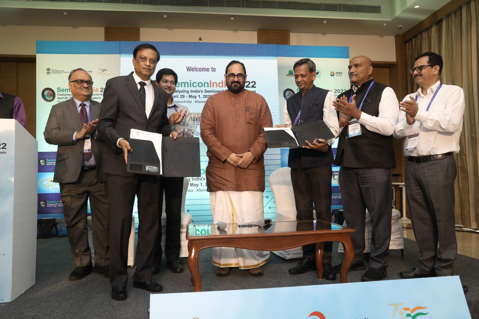
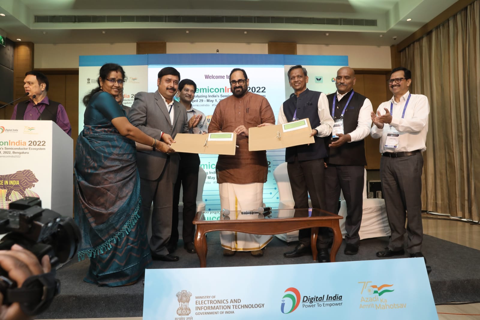
Following MoUs were announced today in backdrop of SemiconIndia 2022:
- India Semiconductor Mission hasannounced an MoU between Cyient, WiSig Networks and IIT Hyderabadto enable mass production of "5G Narrowband-IoT- the Koala Chip, Architected and Designed in India".
Cyient, a leading India-headquartered globalE-R&D & technology solutions company, has partnered with WiSig Networks, a start-up incubated at IIT Hyderabad, to enable volume production of Koala– NB IoT-SoC (Narrowband-IoT System-on-Chip), designed and architected in India. Volume production of the Koala NB-IoTSoC includes the development of a package, test solution suited for volume production, silicon fabrication, volume testing of the IC, and supply management ofthechip. 5G NB-IoT is a fast growing technology that enables low bit rate IoT applications and extends device battery life by upto 10 years. This chip will be used in many applications such as Smart Meters, Asset tracking, Digital Healthcare and many more.
- MoU between Signal chip Innovations, MeitY and Centre for Development of Advanced Computing (C-DAC) for not only design and manufacture but also deployment and maintenance of 10 Lakh Integrated NavIC (Navigation with Indian Constellation) and GPS Receivers. Signalchip, an Indian Fabless semiconductor company has developed “Agumbe” series of baseband, modem and radio frequency (RF) chipsets for 5G/4G networks with integrated support for global navigation satellite systems including NavIC.
These multi-standard chipsets can serve as base station chipset for a wide range of form factors from low-cost indoor small cells to high performance base stations. They have been designed to be suitable for low-cost and low-power systems. They already support positioning using satellite navigation system, including NavIC, to enable several network features.Signalchip has invested and developed almost all the IPs in these chipsets indigenously. Leveraging the IPs created for these chipsets allows Signalchip to quickly build chipsets specifically optimized for navigation systems. The NavIC chipset that will be developed can be used in any device requiring navigation capabilities like mobile phones, vehicles with built-in navigation (e.g. electric vehicles) and tracking devices. They can also be used in low power IoT devices in combination with other technologies like NB-IoT.
- Partnership was announced with Synopsys, Cadence Design Systems, Siemens EDA and Silvaco for making available their Electronic Design Automation (EDA) tools & design solutions for Chips to Startup (C2S) Programme being implemented by CDAC, a scientific society under Ministry of Electronics and IT, Govt. of Indiaat 100+ Institutions for 5 years.
Chips to Startup (C2S) Programme of MeitYaims to create85,000 specialized engineersat B.Tech, M.Tech, PhD level forexpanding Indian Semiconductor talent in the area of VLSI and Embedded System Design at 100+ institutions across the country. Under C2S Programme, the access to leading EDA Tools & design solution from Synopsys, Siemens-EDA, Cadence Design Systems and Silvacowill enable students and researchers to use Industry Grade semiconductor chip design flows and methodologies thereby generating specialized manpower for Semiconductor Design Industry.
- An MoU was announced between Semiconductor Research Corporation (SRC) USA and IIT Bombay to focus on bringing together SRC's industry experts and India's R&D talent to create a compelling industry driven world-class R&D program.
SRC is a world-renowned, high technology-based consortium that serves to enable collaboration between technology companies, academia, government agencies, and SRC’s highly regarded engineers and scientists. IIT Bombay is a premier Institute of National importance with major thrusts in education and innovation in technology, circuits and systems. The MoU signed between SRC and IIT Bombay is focused on bringing together SRC's industry experts and India's R&D talent to create a compelling industry driven world-class R&D program. Through this program, SRC will engage with Indian academia through a public-private partnership (PPP) model co-funded by MeitY. Such industry-driven R&D in semiconductors is the need of the hour as India embarks on the journey to semiconductor manufacturing ecosystem development and technology leadership.
- MeitY announced that Prof. Rao Tummala from Georgia Tech University, USA has consented to be a part of the Advisory Committee of India Semiconductor Mission.
· Prof Rao is a Distinguished and Endowed Chair Professor and Director Emeritus at Georgia Tech in the USA. He is well known as an industrial technologist, technology pioneer and educator.
· Prior to joining Georgia Tech in 1993, he was an IBM Fellow and Director of Advanced Packaging Lab (APTL), pioneering such major technologies as the industry’s first plasma display.
· He is the father of the System-on-Package (SOP) concept vs. System-on-chip (SOC.) by the industry.
· As an educator, Prof. Tummalahas been instrumental in setting up the largest and most comprehensive Academic Center funded by NSF as the first and only NSF Engineering Research Center in Electronic Systems Packaging at Georgia Tech.
· He has authored many books and received countless awards and recognitions.
· He is a distinguished Alumni of the Indian Institute of Science, Bangalore and University of Illinois and Distinguished Faculty of Georgia Tech.
· He has been a consultant and advisor to many Fortune 500 semiconductor and systems companies.
- MoU between Global Institute of Electrical and Electronics Engineers (IEEE India) and Centre for Development of Advanced Computing (C-DAC) was announcedfor skill and technical standards development in semiconductor electronics focusing on VLSI design and Electromagnetic interference (EMI)/ Electromagnetic compatibility (EMC).
The Agreement between IEEE and C-DAC will be used to create specific blended learning programs in the area of semiconductor technologies, cybersecurity; standardization activities; outreach and skill development. CDAC has specific activities focused on skilling, outreach and technology development in the area of semiconductor technologies, IoT and cybersecurity. This will strengthen the semiconductor chip design ecosystem in the country and facilitating access to semiconductor design infrastructure for the start-ups and MSMEs.
- MeitY announced an MoU between Atal Community Innovation Center-Kalasalingam Innovation Foundation (ACIC-KIF) and Centre for Development of Advanced Computing (C-DAC) for collaborative R&D, Product development and Trainings in the areas of semiconductor technologies, Power electronics, Energy harvesting, Electric vehicles etc.
This will provide research and innovation capabilities to rural industries without access to semiconductor facilities. In addition, skill development initiatives in various semiconductor and allied areas will be carried out enabling appropriate manpower availability creating packets of excellence.
RKJ/M
(Release ID: 1821809)
Visitor Counter : 3639