Ministry of Electronics & IT
Government of India is democratizing chip design amongst Indian Universities with access to industry-grade Electronic Design Automation (EDA) tools and Multi-project Wafer (MPW) fabrication services
122 design tapeouts by 46 Institutions across the country in 5 MPW Shuttles organized in past one year
175 Lakh hours of EDA tools usage by over 380+ organizations supported by the ChipIN Centre
‘This kind of large-scale semiconductor development ecosystem is unique to India’, says Union Minister Ashwini Vaishnaw
Posted On:
29 NOV 2025 8:28PM by PIB Delhi
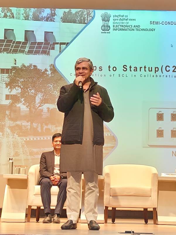
Union Minister for Electronics & Information Technology, Shri Ashwini Vaishnaw, handed over 28 chips fabricated at Semiconductor Laboratory (SCL) Mohali (including 600 bare dies & 600 packaged chips) by students from 17 academic institutions under the Chips to Start-up (C2S) Programme. The chip handover ceremony was organized during his visit to the Semiconductor Laboratory (SCL), Mohali, on 28th November 2025 to review the progress of work and ongoing modernisation activities.
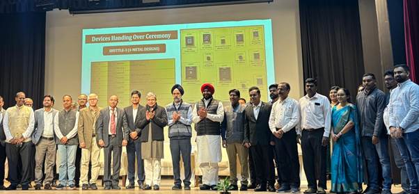
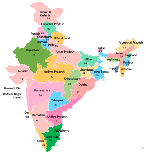
During the ceremony, the Minister stated that India is rapidly emerging as a distinctive leader in the global semiconductor landscape. Today, institutions across the country have access to some of the world’s most advanced design technologies, creating a large-scale semiconductor development ecosystem that is unique to India. The following image details out the number of organizations supported with EDA tools in different states of the country:
Director General, SCL and the team gave a detailed presentation on the chip design and fabrication process adopted under C2S Programme leveraging SCL and ChipIN Centre collaborative approach under C2S Programme, on this occasion.
About ChipIN Centre:
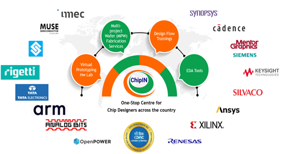
ChipIN Centre, one of the largest facilities established at C-DAC Bangalore, offers an extensive range of semiconductor design workflows and solutions, striving to bring national chip design infrastructure directly to the semiconductor design community across the country. It is a centralized facility which hosts the most advanced tools for the entire chip design cycle.
It also offers compute and hardware infrastructure, IP cores, and mentorship to provide comprehensive services for design fabrication at the SCL foundry and packaging to academic institutions under C2S (Chips to Start-up) Programme of Ministry of Electronics and Information Technology, Government of India.
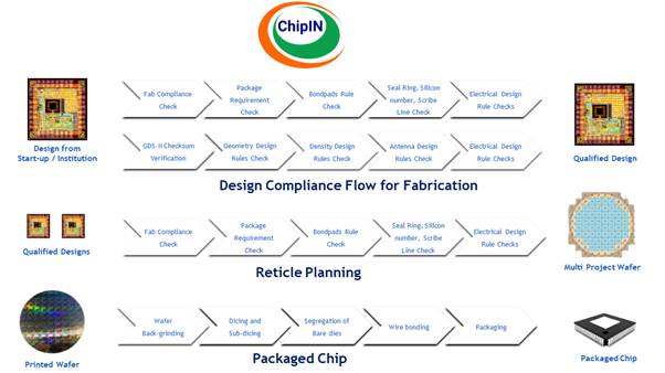
The ChipIN Centre collects chip designs created by students from C2S Programme institutions. Every three months, these designs are grouped together and sent to SCL Mohali for fabrication using 180 nm technology. The ChipIN Centre conducts fab-compliance checks, working closely with students and institutions through iterative feedback and design revisions. Once approved, the designs are combined onto a single mask (MPW reticle) by ChipIN Centre, which saves both time and cost by manufacturing multiple designs in a single run. SCL Mohali then fabricates, packages, and delivers the chips back to the students.
In the past year, ChipIN Centre organized 5 such MPW shuttle runs for fabrication of designs at SCL under C2S Programme. A total of 122 designs were submitted by 46 institutions across India. Out of these, SCL has successfully fabricated 56 student-designed chips and delivered them to the respective institutions. Shuttle-wise information is as below with consolidated details of design at https://c2s.gov.in/MPW_Services.jsp :
| |
|
Tape out date
|
Designs
|
Institutions
|
|
1
|
MPW Shuttle-I
|
06th Dec 2024
|
20
|
17
|
|
2
|
MPW Shuttle-II
|
28th Feb 2025
|
14
|
12
|
|
3
|
MPW Shuttle-III
|
31st May 2025
|
22
|
15
|
|
4
|
MPW Shuttle-IV
|
31st Aug 2025
|
38
|
20
|
|
5
|
MPW Shuttle-V
|
30th Nov 2025
|
28
|
24
|
|
|
Total
|
|
122 design tapeouts
|
46 individual institutions
|
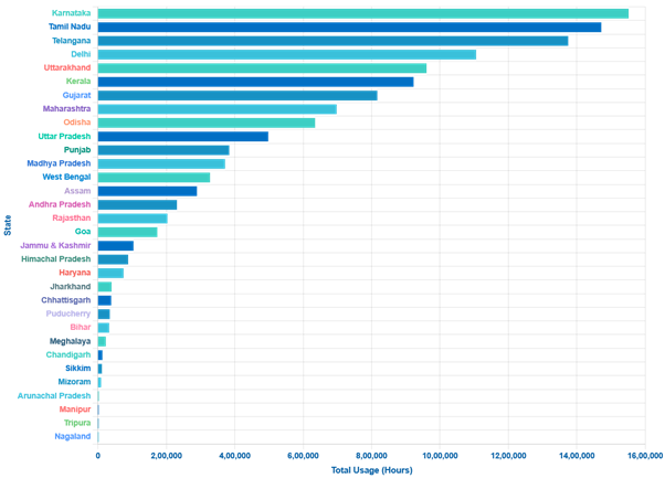
With 5 shuttles successfully concluded in past one year for SCL Mohali, ChipIN Centre is rapidly advancing its capability to act as value chain aggregator (VCA) for advance nodes too. During these design tapeouts and related teaching, instruction, and research activities at supported institutions, over 1 lakh students from participating institutions used more than 125 lakh hours of EDA tools. In addition, the ChipIN Centre is supporting over 90 startups, which used about 50 lakh hours of EDA tools during the same period. This brings the total EDA tool usage to more than 175 lakh hours, making it one of the world’s largest centralized chip-design user facilities. Following is the State-wise EDA tools usage at various academic institutions:
During the ceremony, Shri Ashwini Vaishnaw mentioned that this progress reflects the expansive vision of the Prime Minister Narendra Modi, whose directive is clear: India must build capabilities of such scale and strength that, within the next few years, the nation establishes itself as a major global semiconductor power. He also mentioned that the aim is to ensure that we do not depend on anyone else for our strategic needs and to become self-reliant in our strategic sectors and to use indigenous chips. In this strategy, SCL will play a very significant role.
*****
MSZ
(Release ID: 2196422)
Visitor Counter : 6073