PIB Backgrounder
India Building Semiconductor Future
Emerging Capabilities Across Design, Manufacturing, Packaging, Materials and Talent
Posted On:
17 SEP 2026 12:08PM by PIB Delhi
|
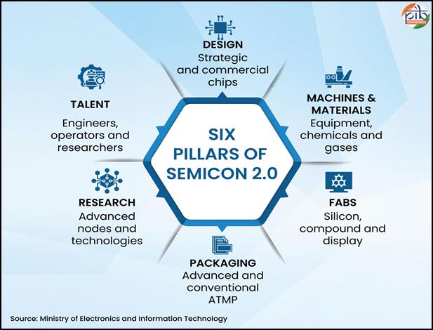
Building on the successful implementation of Semicon 1.0, the Union Cabinet approved Semicon 2.0 on 15 July 2026 with an outlay of Rs 1,27,500 crore. While the first phase laid the foundation for India's semiconductor manufacturing ecosystem, Semicon 2.0 advances the next phase through six strategic pillars. These include research and development, chip design, machines and materials, setting up more fabs, talent development, and further strengthening the ATMP/OSAT industry. It will position India as a trusted global semiconductor hub and advance the vision of Viksit Bharat.
|
Setting the Context
Semiconductors are the building blocks of modern technology and a foundation of economic power. They power Artificial Intelligence (AI), telecommunications, electric mobility, defence and advanced manufacturing. Technologies such as the Internet of Things (IoT), 5G/6G, data centres and autonomous vehicles are further driving chip demand. Their availability and technological capabilities will increasingly shape innovation, competitiveness and national technological strength.
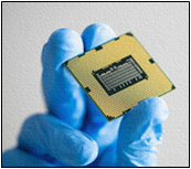
This growing importance is reflected in the rapid expansion of the global semiconductor market. The global semiconductor market grew at a compound annual growth rate (CAGR) of 6.5 per cent between 2014 and 2024. It is projected to grow at 8.5 per cent over the next 5–10 years. However, recent disruptions have exposed vulnerabilities in the interconnected global semiconductor value chain. Geopolitical tensions have further highlighted the risks of supply dependence. Major economies are therefore strengthening domestic semiconductor capabilities to secure their technological and economic interests.
India is also witnessing rapidly rising semiconductor demand. It is projected to reach USD 110 billion by FY2030 and exceed USD 200 billion by FY2035, while domestic manufacturing remains at a nascent stage. India spent almost USD 150 billion on semiconductor product imports during FY17–FY25. Imports grew at a CAGR of 23 per cent during this period. If this trend continues, annual imports could reach USD 240 billion by 2035. Building a comprehensive semiconductor ecosystem is therefore an urgent national priority. The Government of India is strengthening this ecosystem to advance self-reliance, security, skills and technological competitiveness.
|
SEMICON 2026: Catalyzing India’s Semiconductor Ecosystem
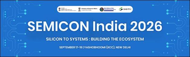
Semiconductors form the core of modern electronic systems. Building a strong semiconductor ecosystem is therefore essential for technological resilience, economic security and national self-reliance. Recognising this strategic importance, the Government of India is strengthening the semiconductor ecosystem through policy support, infrastructure and global partnerships. In this endeavours, SEMICON India 2026, themed “Silicon to Systems: Building the Ecosystem,” was inaugurated by Prime Minister Shri Narendra Modi at Yashobhoomi, New Delhi, on 17 September 2026. Being held from 17 to 19 September 2026, the SEMICON 2026 brings together global industry leaders, policymakers, investors, academia and start-ups. It provides a platform to advance India’s semiconductor ambitions and strengthen the ecosystem across the entire value chain. Click To Explore Agenda
|
What is a Semiconductor?
A semiconductor is a material whose electrical conductivity can be controlled. Conductors such as copper allow current to flow easily, while insulators strongly resist it. Semiconductor materials can be engineered to switch, amplify, sense or control electrical signals. A transistor is a microscopic electronic switch. Modern integrated circuits place millions or billions of transistors and other components on a small chip. Their coordinated switching makes computing, communications, sensing, memory and power management possible.
Most modern electronic devices depend on semiconductors. Smartphones, computers, medical equipment, automobiles, defence systems, satellites and data centres use semiconductor-based components. In simple terms, semiconductors are the building blocks of modern electronics.
From Silicon to a Semiconductor Chip
Silicon is the most widely used semiconductor material. It is obtained from silica, which occurs abundantly in sand. Chip manufacturing begins with highly purified silicon, which is formed into cylindrical ingots. These ingots are sliced into thin wafers and polished. Inside fabrication plants, wafers undergo hundreds of carefully controlled processes. These include deposition, photolithography, etching and ion implantation.
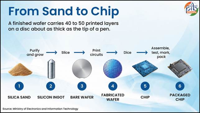
Together, these processes create the intricate structures that form billions of transistors and other components. During photolithography, patterns are transferred onto the wafer using light. These patterns define structures that ultimately form transistors, interconnects and other parts of a chip. Transistors are the microscopic electronic switches on the chip that control the flow of electrical current. The process is repeated across multiple layers to build complex integrated circuits.
Finished semiconductor devices then undergo Assembly, Testing, Marking and Packaging (ATMP) or Outsourced Semiconductor Assembly and Test (OSAT) processes. Packaging protects the chip and enables it to connect with other electronic components. Testing ensures that the finished devices meet required performance and quality standards.
Understanding Semiconductor Node
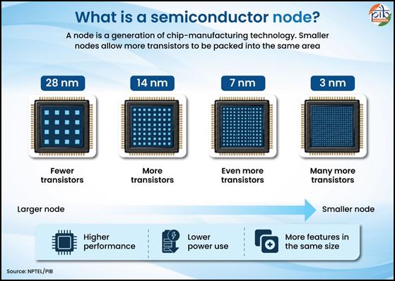
A semiconductor node identifies a generation of manufacturing technology. Historically, labels such as 90 nm, 45 nm and 28 nm tracked particular physical dimensions. Today, node names function mainly as shorthand for a process generation. A smaller node can enable higher transistor density, better performance or lower energy use, but the result also depends on circuit design, materials, packaging and the intended application. Advanced nodes attract attention because they support high-performance computing and leading-edge processors. Mature nodes remain essential for automobiles, industrial electronics, telecommunications, power systems and many consumer products. India is now building capabilities that extend from established nodes towards more advanced semiconductor technologies.
Why Semiconductors: A Strategic Perspective
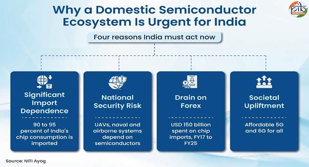
Semiconductors have emerged as a strategic resource for economic growth, technological leadership and national security. Today, Taiwan, South Korea, Japan, China and the United States dominate global semiconductor manufacturing. Taiwan alone accounts for over 60% of global chip production and nearly 90% of advanced chips. This concentration has highlighted the need for secure, diversified and resilient semiconductor supply chains. For India, domestic semiconductor capabilities are more than an industrial opportunity. They are essential for reducing import dependence, strengthening national security and creating high-value employment. They can also deepen technological self-reliance and reduce vulnerabilities across strategic sectors. No single country controls the complete semiconductor value chain. Different economies lead in chip design, fabrication, equipment, materials, memory and packaging. This specialisation has improved efficiency, but it also creates concentration risk. India’s policy therefore focuses on trusted partnerships alongside stronger domestic capacity.
|
Semiconductors Power India’s Strategic Missions
- Semiconductor Laboratory (SCL), Mohali develops flight-grade chips for satellites and launch vehicles, designed to withstand extreme space conditions.
- Chandrayaan-3’s lander carried an Indian-made camera chip, supporting the lander’s imaging systems.
- SCL’s Vikram processor is used in satellite launch vehicles and rockets.
- Aditya-L1, India’s mission to study the Sun, uses radiation-hardened ADC chips developed by SCL.
|
India’s Emerging Semiconductor Ecosystem
India’s semiconductor journey has evolved from building strategic capabilities to creating a broader domestic ecosystem. Early institutions such as the Semiconductor Laboratory (SCL) laid the groundwork, while recent policy interventions have accelerated investment, innovation and talent development. These efforts are positioning India to participate across the semiconductor value chain.
Semicon 1.0: Laying the foundation
The Government of India approved Semicon 1.0 in December 2021, with an outlay of ₹76,000 crore. It aimed to establish a domestic semiconductor and display manufacturing ecosystem. The programme introduced dedicated Schemes for setting up Semiconductor Fabs and Display Fabs. It also introduced the Scheme for setting up Compound Semiconductors, Silicon Photonics, Sensors and Semiconductor ATMP/OSAT facilities. Additionally, the Design Linked Incentive (DLI) Scheme strengthened India's semiconductor design capabilities. Together, these schemes established the foundation across chip design, fabrication, packaging and related technologies.
|
Semicon 1.0: Key Achievements
- Twelve semiconductor manufacturing units approved, carrying cumulative investment of over Rs 1.64 lakh crore.
- These include one silicon fab, one silicon carbide fab, one Gallium Nitride Micro LED Display Fab and nine ATMP/OSAT units.
- Units are located in Gujarat, Assam, Uttar Pradesh, Odisha, Punjab and Andhra Pradesh. Five units have commenced commercial production.
- Twenty-four chip design projects approved, with a total value of about Rs 900 crore.
- More than 1 lakh engineers from 500 organizations across the country, including 400 academic institutions and 100 start-ups have been provided access to advanced chip-design tools.
- Together, our organizations have developed more than 300 chip designs.
- India has established semiconductor cooperation with partners including the United States, Japan, the European Union, Singapore and the Netherlands.
- India signed a Joint Declaration of Intent on an India-Germany Semiconductor Ecosystem Partnership during the German Chancellor's visit from 12 to 13 January 2026, and joined Pax Silica at the India AI Impact Summit in February 2026.
- India hosts about 7% of the world’s Global Capability Centres (GCCs) of Semiconductor domain and employs nearly 20% of the global semiconductor chip design workforce.
|
Semicon 2.0: Building the Complete Ecosystem
Building on the foundation laid by Semicon 1.0, the Government of India approved Semicon 2.0 in July 2026 with a total outlay of ₹1,27,500 crore. The programme seeks to provide sustained and long-term support to India’s semiconductor sector. It aims to deepen the capabilities created under Semicon 1.0 and accelerate the growth of a globally competitive semiconductor ecosystem. Semicon 1.0 concentrated mainly on fabs and ATMP/OSAT plants. Semicon 2.0 adds machines and materials, design, research and talent to the mission. Together, the two phases span the chain from raw materials to finished chips.
Semicon 2.0 rests on six pillars: design, machines and materials, setting up new fabs, further advanced packaging, research and talent development. Its purpose is to build the complete chip value chain within the country, and not merely its closing stages. This effort carries India towards supply chain resilience, strategic autonomy and high-value employment in a technology that now underpins every modern industry.
Key Supporting Policy Ecosystem[1]
India’s semiconductor ambitions are supported by a progressive policy ecosystem spanning manufacturing, infrastructure, investment, research and talent development. These measures have steadily strengthened the electronics value chain and created a foundation for semiconductor self-reliance.
- National Policy on Electronics (NPE) 2019 – Established the overarching framework for Electronics System Design and Manufacturing (ESDM), including core components such as chipsets.
- Scheme for Promotion of Manufacturing of Electronic Components and Semiconductors (SPECS) (2020) – Provides capital expenditure linked incentive for domestic manufacturing of components, sub-assemblies and semiconductors in order to strengthen the electronics manufacturing ecosystem in the country
- Modified Electronics Manufacturing Clusters Scheme (EMC 2.0) (2020) – Supports world-class infrastructure, common facilities and plug-and-play facilities for electronics manufacturing.
- Production Linked Incentive (PLI) Scheme for Large Scale Electronics Manufacturing (2020) – Provides production link incentive to boost domestic manufacturing and attract large investments in mobile phones and components manufacturing.
- Production Linked Incentive (PLI) Scheme 2.0 for Information Technology (IT) Hardware (2023) – To boost domestic manufacturing of IT Hardware and attract large investments in its value chain. It promotes domestic manufacturing of laptops, tablets, All-in-One Personal Computers and servers.
- Electronics Components Manufacturing Scheme (2025) – With an enhanced outlay of ₹40,000 crore (Budget 2026–27), to develop robust component manufacturing ecosystem by attracting investments across the value chain, leading to increase in Domestic Value Addition (DVA).
- Mobile Phone Manufacturing Scheme (2026) – Aims to increase global competitiveness by further enhancing the scale, deepening the mobile manufacturing supply chain through higher domestic value addition (DVA) and stronger domestic manufacturing capabilities, and supporting Indian mobile brands.
- Research, Development and Innovation Scheme – Supports eligible research projects under Semicon 2.0 and strengthens domestic semiconductor innovation.
- 100% Foreign Direct Investment (FDI) Policy for Electronics Manufacturing – Facilitates global investment and technology partnerships while integrating India with global electronics and semiconductor value chains.
These initiatives are creating the industrial base, market demand and investment environment needed for a resilient semiconductor ecosystem. They complement flagship semiconductor initiatives and advance India’s goal of becoming a global electronics and semiconductor hub.
Towards an Advanced & Self-Reliant India
India’s semiconductor story has advanced rapidly in a short period. In 2021, the country had no commercial chip plant. By 2026, twelve units stand approved, and five are in production. Students across hundreds of colleges are now designing chips. Semicon 2.0 is the natural next chapter in this account. It does not begin afresh. It takes a functioning ecosystem and completes it. Machines, materials, design, research and talent now join fabs and packaging. The road ahead is demanding. Chip manufacturing ranks among the most complex industries in the world. It requires patience, precision and steady policy support. Semicon 2.0 provides that support for the long term. For citizens, the gain will be quiet but real. Devices will be manufactured more fully within India. Critical systems will depend less upon distant supply chains. Young engineers will find high-value work closer to home. A small chip carries a large promise. India has resolved to build it at home.
References
Ministry of Electronics and Information Technology
India Semiconductor Mission
Semiconductor Laboratory
Union Cabinet
Press Information Bureau (Factsheets and Backgrounders)
NITI Aayog
Indian Institute of Technology Madras
Indian Institute of Technology Kanpur
https://sathee.iitk.ac.in/sathee-jee/ncert-books/jee-ncert-books/jee-nb-phy-12/phy-12-chapter-14-semiconductor-electronics-materials-devices-and-simple-circuits/
Union Minister for Electronics and Information Technology
India Building Semiconductor Future
*****
PIB Research
(Release ID: 2311220)
Visitor Counter : 499